Productive process
Technical department
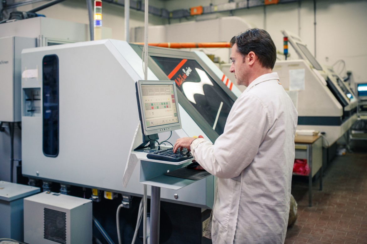
The technical department receives Gerber files developed by designers, and examines their manufacturability in conjunction with the Quality Manager, who monitors quality throughout the entire production process. The technical department sets up the CAD/CAM configurations for all the machines, according to a lean, logical production programme that has been consolidated over many years.
Laminate and chemical warehouse
The warehouse is managed by means of an MRP system. Every batch is coded in the business software, which monitors stock turnover. This plays a vital role in maintaining above-standard quality at all times.
Machining department
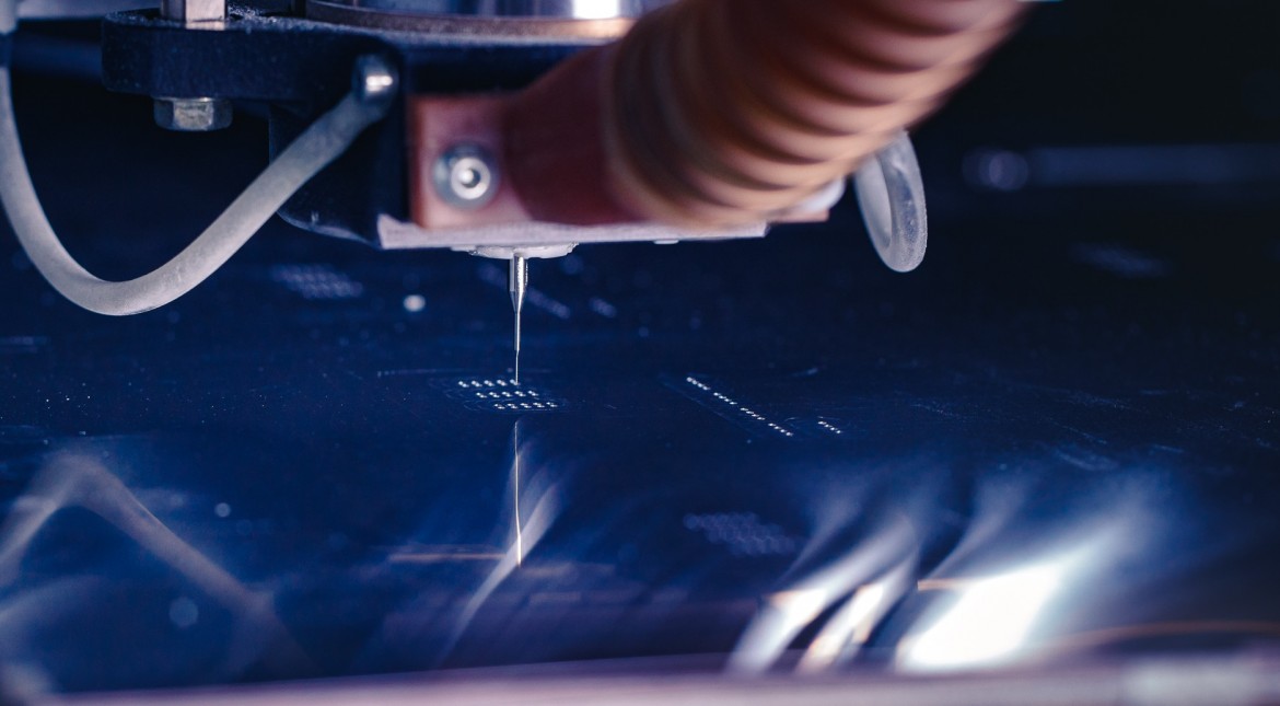
The decision to keep all machining processes together in a single department facilitates monitoring of the progress of PCB production orders. CSM is equipped with CNC drilling machines with 200,000 rpm asynchronous spindles, routers, milling machines for polymeric materials and milling machines for aluminium.
Film plotting and exposure
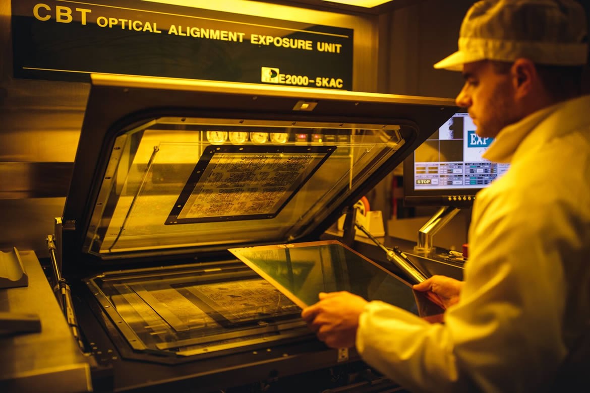
Before preparing the equipment, the customer's requirements are carefully examined to ensure faithful replication of the circuit in terms of quality, quantity and delivery times. The dry-film exposure and lamination process takes place in a climate-controlled yellow room, with air filtration and controlled temperature and humidity. This ensures the dimensional stability of the materials and the production of PCBs with Fine Line tracks of up to 100 microns.
Multi-layer pressing
CSM is equipped with a multi-daylight press for the preparation of multi-layer PCBs. This machine is capable of reaching temperatures of 350°C with a precision of +/- 1 degree at all points. In conjunction with the 20 years' experience of our personnel, this enables us to join different materials to produce increasingly complex PCBs.
Hole metallization
This phase involves electrolytically depositing the quantity of copper required by the customer on the tracks and in the holes.
Alkaline etching
Here the tracks of your PCB take definitive shape. Stringent process control enables us to produce fine lines of consistently high quality.
Solder masking and silkscreening
The solder mask is applied by means of a curtain coater, which deposits a uniform layer of paint across the entire surface. The thickness of the solder mask is determined on the basis of the thickness of copper required by the customer, in full compliance with IPC standards. The resins in question catalyse with the UV radiation and precisely expose the pads for component mounting. A similar process is performed for silkscreening.
Quality Checking
As well as chemical analyses of the operating parameters of the various production processes, we also conduct tests in our laboratories to check the quality of our PCBs. Here we perform metallographic, wettability and thermal stress tests, and mechanical measurements.
The aim of these tests is to ensure that everything we produce meets the highest possible standards of quality.
Surface finish
We use chemical silver as a finish because it has the major benefits of planarity, wettability and absence of thermal stress.
Electrical testing
It is imperative to check the electrical conformity of all PCBs so that any PCB manifesting short circuits or breaks in the tracks can be discarded. All our products are therefore checked with soft-touch top and bottom flying probe automated test equipment (ATE).
Vacuum packing
To safeguard our PCBs against oxygen and adverse weather conditions, we seal them in impermeable shrink-wrap. On express customer request, we can also pack smaller batches than our standard pack.


